The Circuitry
THE CIRCUITRYYour one-stop source for all tech news
HOMETODAYNEWSFEEDEVENTS
BOOKMARKS
RSS
© 2026 The Circuitry
About UsSourcesContactCorrectionsPrivacy
  • Today
  • Feed
  • Events
  • Saved
Scroll for more
Verification
VERIFIEDConfidence: HIGH
Source identified
Claims cross-referenced
No discrepancies found
Fact-check summary

Ars Technica's report on IBM's NanoStack transistor research for sub-1nm nodes aligns with IBM Research publications and papers from the 2025 and 2026 VLSI symposia.

Sourcing
1source

via Ars Technica

Ars Technica · track record
30Stories
100%Verified
130d
All sources →
From The CircuitryWhy The Circuitry

Verified tech news, cross-checked.

Every story is checked against independent sources before it posts — no rumors dressed up as fact.

How we verify →
Home/Tech/IBM reveals nanostack transistor design targeting sub-1nm performance
VERIFIEDBy Xavier Rivera· ·2 min read

IBM reveals nanostack transistor design targeting sub-1nm performance

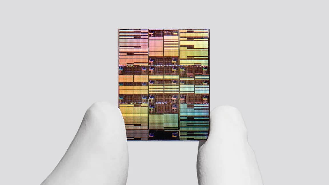
IBM has detailed a nanostack transistor architecture it calls the world’s first sub-1 nanometer chip technology, enabling nearly 100 billion transistors on a fingernail-sized die. The approach is projected to yield 50 percent higher performance or 70 percent better energy efficiency than the prior 2nm generation while delivering a 40 percent SRAM scaling gain for AI workloads.
Source:Ars Technica
Post
IBM reveals nanostack transistor design targeting sub-1nm performance
From The CircuitryWhy The Circuitry

Verified tech news, cross-checked.

Every story is checked against independent sources before it posts — no rumors dressed up as fact.

How we verify →
TL;DRAI · 60 sec read

IBM presents a nanostack transistor design that achieves sub-1-nanometer performance by stacking transistors vertically in an offset pattern. This packs nearly 100 billion transistors on a fingernail-sized surface, nearly doubling density from the 2-nanometer process. The design targets AI data centers with 50 percent higher performance or 70 percent better efficiency.

A fresh chip design unveiled by IBM reportedly packs nearly 100 billion transistors onto a surface no larger than a human fingernail, almost doubling the density achieved in the firm’s last generation of technology. The company positions the advance as the “world’s first sub-1 nanometer chip technology” developed specifically for AI data centers.

Vertical stacking overcomes physical limits. The nanostack approach places transistors atop one another in an offset pattern, allowing far more of them to occupy the same area. It extends the nanosheet devices that first appeared in IBM’s 2-nanometer process launched in 2021.
Feature sizes stopped matching node numbers after the 180-nanometer era of the 1970s and 1980s.
At its core, the architecture bonds two transistors together vertically. Each transistor contains three nanosheets measuring 5 nanometers thick—roughly 15 rows of silicon atoms—with approximately 9 nanometers between neighboring sheets.

Projected gains aim at AI-era demands. Technical papers released by the company forecast that the new layout can deliver 50 percent higher computing performance or 70 percent greater energy efficiency relative to its 2-nanometer predecessor. IBM first presented the nanostack concept at the 2025 IEEE Symposium on VLSI Technology and Circuits held in Kyoto, Japan.
From The CircuitryThe Feed — live briefs across tech, all day.See what’s happening →
Separate work shown at the VLSI 2026 symposium indicated a 40 percent scaling improvement for SRAM. The gain stems from a staggered-channel layout inside SRAM bit cells—each built from six transistors—that shrinks cell height by 40 percent and fits more memory in the same footprint.
The improvement arrives after SRAM scaling has slowed sharply; the step from 3-nanometer to 2-nanometer processes delivered only a few percent density gain.
SRAM density boost addresses AI needs. That extra memory capacity matters because SRAM handles rapid yet power-hungry read and write cycles required by many AI tasks. The improvement arrives after SRAM scaling has slowed sharply; the step from 3-nanometer to 2-nanometer processes delivered only a few percent density gain.

Node labels no longer reflect true size. IBM calls the technology a 0.7-nanometer or 7 angstrom node, even though modern process names have long since decoupled from actual physical dimensions. Feature sizes stopped matching node numbers after the 180-nanometer era of the 1970s and 1980s.
From The CircuitryWhy The Circuitry

Verified tech news, cross-checked.

Every story is checked against independent sources before it posts — no rumors dressed up as fact.

How we verify →
“It’s not just an incremental step, it’s a meaningful leap forward,” said Jay Gambetta, director of IBM Research and IBM Fellow. He added that the platform “pointing to a future where computing becomes significantly more powerful without a corresponding increase in energy.”
Why this mattersAI · ~100 words

Tap a lens to see what this story means for you.

Morning Brief

Liked this? The Brief brings you the whole day in tech, verified, every morning.

Two minutes, free forever. What's in The Brief →

Reader-supported
DonateBuy me a coffee →Follow@thecircuitry_ →Follow@thecircuitry.to →
HELP US IMPROVE
From The Circuitry

See what’s happening right now

The Feed runs all day — short, verified briefs the moment they break.

Open the Feed →
From The Circuitry

Follow @thecircuitry_

Every story we publish, as it happens. No noise between.

Follow on X ↗On Bluesky ↗

Reader-supported

The Circuitry is a passion project I've always wanted to build, and I love the work behind it.

Running it costs real money. APIs, hosting, time. To keep improving the site and growing this into something useful for everyone, those costs have to be covered.

Any contribution is appreciated. If not, no pressure. Thanks for reading.

Buy me a coffee
IBMsemiconductorsAI hardware
More fromArs Technica
  • Vendors object to Spirit Airlines selling operational data to Google in bankruptcy

    Tech · 28d
  • Twitch adds opt-out for Amazon’s generative AI training on user content

    Tech · 1mo
  • Aptoide becomes first rival app store hosted in Google Play

    Tech · 1mo
More inTech
  • SpaceX agrees to buy 800 MHz spectrum for Starlink Mobile

    Tech · 11h
  • Microsoft discloses CVE-2026-83947 in Azure Event Grid

    Tech · 11h
  • Critical CVE-2026-77900 Hits Microsoft Azure App Service for Linux

    Tech · 11h
SupportThe Work

The Circuitry is reader-supported. If you find the daily brief useful, you can buy me a coffee to keep it going.

Buy a coffee →
From The CircuitryWhy The Circuitry

Verified tech news, cross-checked.

Every story is checked against independent sources before it posts — no rumors dressed up as fact.

How we verify →

MORE IN THIS BEAT

All Tech →
  • Tech· 

    GlobalFoundries signs $2B TSMC deal for US silicon interposers

    GlobalFoundries signed a multi-year US$2 billion agreement with TSMC on October 8, 2026 to manufacture silicon interposers at its Malta, New York fab. The deal creates the first US-based source of silicon interposers for TSMC's CoWoS advanced packaging ecosystem.

  • Tech· 

    Critical CVE-2026-16823 hits IBM Security Verify Access

    IBM Security Verify Access 10.0 through 10.0.9.2 and IBM Verify Identity Access 11.0 through 11.0.3 contain critical authentication bypass flaw CVE-2026-16823. The NVD rates it 9.1 and warns of remote exploitation without credentials.

  • Tech· 

    IBM patches nine Guardium Data Protection flaws

    IBM has released patches addressing nine vulnerabilities in Guardium Data Protection across versions 12.0 through 12.2.2. Two of the flaws are rated critical and could allow remote attackers to seize control of edge clusters or execute scripts in user browsers.

  • Tech· 

    IBM Patches 40 DataPower Gateway Flaws, Seven Rated Critical

    IBM has fixed 40 vulnerabilities in DataPower Gateway, seven of them rated critical at CVSS 9.3 to 9.8, including remote code execution bugs and an LDAP flaw that accepts empty passwords for admin access. IBM says to upgrade to 10.5.0.23, 10.6.0.11 or 11.0.0.3.

  • Tech· 

    Marvell lifts 2028 revenue target to approximately $20B on AI connectivity

    Marvell Technology raised its fiscal 2028 revenue outlook to approximately $20 billion and set a fiscal 2031 target of $70-90 billion. The increases reflect expected growth in AI networking and optical connectivity demand.