The Circuitry
THE CIRCUITRYYour one-stop source for all tech news
HOMETODAYNEWSFEEDEVENTS
BOOKMARKS
RSS
© 2026 The Circuitry
About UsSourcesContactCorrectionsPrivacy
  • Today
  • Feed
  • Events
  • Saved
Scroll for more
Verification
VERIFIEDConfidence: HIGH
Source identified
Claims cross-referenced
No discrepancies found
Fact-check summary

ASML's July 15 press release, corroborated by Reuters and Wccftech, confirms Intel Foundry is the first to enter high-volume manufacturing of Panther Lake processors using High-NA EUV on its 18A node.

Sourcing
1source

via DigiTimes Asia

DigiTimes Asia · track record
50Stories
100%Verified
830d
All sources →
Markets
INTC···

Live quote · not investment advice

From The CircuitryWhy The Circuitry

Verified tech news, cross-checked.

Every story is checked against independent sources before it posts — no rumors dressed up as fact.

How we verify →
Home/Tech/Intel Ships First High-NA EUV Logic Product for Panther Lake
VERIFIEDBy Xavier Rivera· ·1 min read

Intel Ships First High-NA EUV Logic Product for Panther Lake

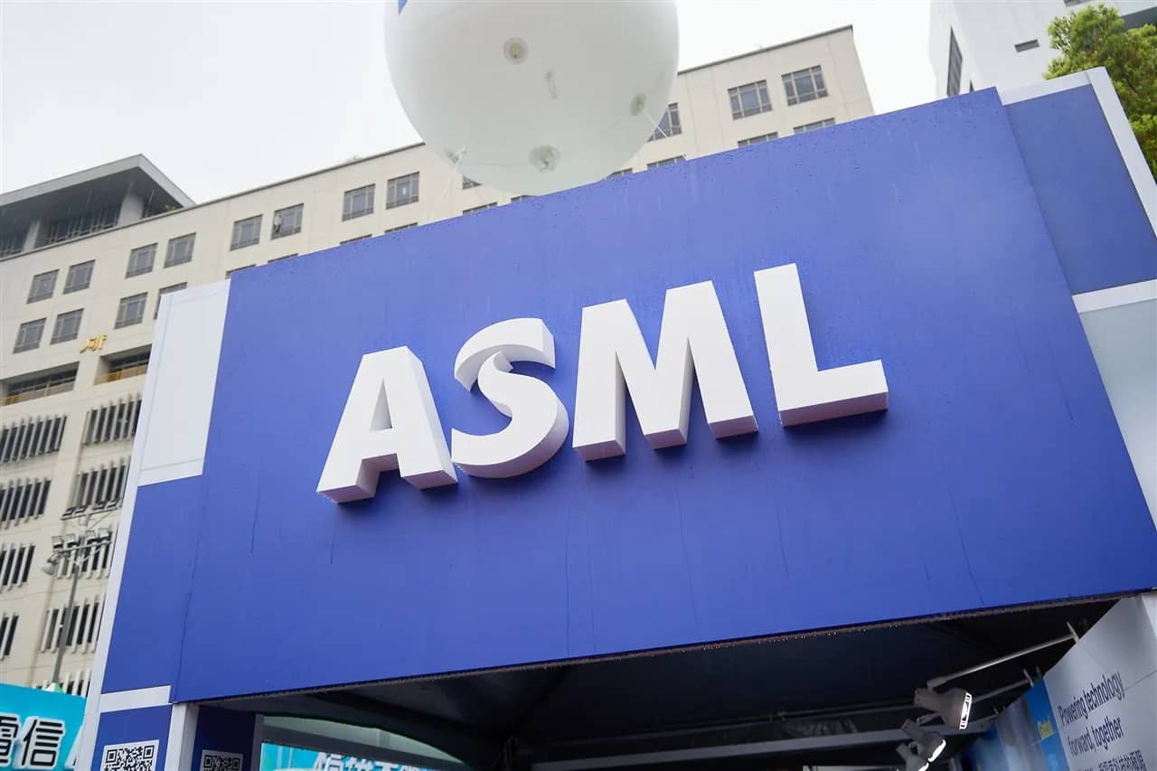
ASML confirmed on July 15 that Intel Foundry shipped the first high-volume logic product made with High-NA EUV lithography for Panther Lake. The milestone advances commercial readiness of the technology while ASML prepares TSMC and Samsung for wider adoption.
Source:DigiTimes Asia
Post
Intel Ships First High-NA EUV Logic Product for Panther Lake
From The CircuitryWhy The Circuitry

Verified tech news, cross-checked.

Every story is checked against independent sources before it posts — no rumors dressed up as fact.

How we verify →
TL;DRAI · 60 sec read

Intel Foundry ships the first high-volume logic product manufactured using High-NA EUV lithography for its Panther Lake processors. ASML confirmed this commercial milestone on July 15. The milestone advances semiconductor manufacturing precision and positions Intel ahead of TSMC and Samsung as ASML prepares them for the technology's next phase of adoption.

ASML has confirmed that Intel Foundry is the first company to ship a high-volume logic product manufactured using High-NA EUV lithography.

Intel achieves commercial milestone with High-NA EUV. The confirmation came on July 15 as Intel qualifies the technology for its Panther Lake processors. This marks the first commercial readiness of ASML's most advanced lithography system in high-volume logic production.
This marks the first commercial readiness of ASML's most advanced lithography system in high-volume logic production.

The milestone positions Intel Foundry ahead in the deployment of High-NA EUV tools.

ASML advances next-wave preparation for TSMC and Samsung. The Dutch equipment maker is preparing TSMC and Samsung for the subsequent phase of High-NA EUV adoption. These efforts follow Intel's qualification and aim to broaden industry use of the technology.
From The CircuitryThe Feed — live briefs across tech, all day.See what’s happening →

ASML's High-NA EUV lithography represents a key advancement in semiconductor manufacturing precision. The system enables finer patterning required for future chip generations. Intel's Panther Lake chips now incorporate this capability in production volumes.
Intel's Panther Lake chips now incorporate this capability in production volumes.

Industry context centers on logic chip manufacturing leadership. Intel Foundry's achievement underscores its progress in process technology amid competition from foundry peers. The July 15 confirmation highlights the transition from development to commercial shipment for High-NA EUV.
From The CircuitryWhy The Circuitry

Verified tech news, cross-checked.

Every story is checked against independent sources before it posts — no rumors dressed up as fact.

How we verify →
TSMC and Samsung are positioned to follow Intel's lead in integrating the lithography tools. Their preparation by ASML indicates an accelerating rollout across major semiconductor players. The development signals broader availability of High-NA EUV for logic products in coming cycles.
Why this mattersAI · ~100 words

Tap a lens to see what this story means for you.

Morning Brief

Liked this? The Brief brings you the whole day in tech, verified, every morning.

Two minutes, free forever. What's in The Brief →

Reader-supported
DonateBuy me a coffee →Follow@thecircuitry_ →Follow@thecircuitry.to →
HELP US IMPROVE
From The Circuitry

See what’s happening right now

The Feed runs all day — short, verified briefs the moment they break.

Open the Feed →
From The Circuitry

Follow @thecircuitry_

Every story we publish, as it happens. No noise between.

Follow on X ↗On Bluesky ↗

Reader-supported

The Circuitry is a passion project I've always wanted to build, and I love the work behind it.

Running it costs real money. APIs, hosting, time. To keep improving the site and growing this into something useful for everyone, those costs have to be covered.

Any contribution is appreciated. If not, no pressure. Thanks for reading.

Buy me a coffee
SemiconductorsIntelASMLEUV Lithography
More fromDigiTimes Asia
  • GlobalFoundries signs $2B TSMC deal for US silicon interposers

    Tech · 8h
  • Marvell lifts 2028 revenue target to approximately $20B on AI connectivity

    Tech · 2d
  • Report: Biren Technology Prepares BR20X GPU for Mass Production

    Tech · 6d
More inTech
  • SpaceX agrees to buy 800 MHz spectrum for Starlink Mobile

    Tech · 11h
  • Microsoft discloses CVE-2026-83947 in Azure Event Grid

    Tech · 11h
  • Critical CVE-2026-77900 Hits Microsoft Azure App Service for Linux

    Tech · 11h
SupportThe Work

The Circuitry is reader-supported. If you find the daily brief useful, you can buy me a coffee to keep it going.

Buy a coffee →
From The CircuitryWhy The Circuitry

Verified tech news, cross-checked.

Every story is checked against independent sources before it posts — no rumors dressed up as fact.

How we verify →

MORE IN THIS BEAT

All Tech →
  • Tech· 

    GlobalFoundries signs $2B TSMC deal for US silicon interposers

    GlobalFoundries signed a multi-year US$2 billion agreement with TSMC on October 8, 2026 to manufacture silicon interposers at its Malta, New York fab. The deal creates the first US-based source of silicon interposers for TSMC's CoWoS advanced packaging ecosystem.

  • Tech· 

    Marvell lifts 2028 revenue target to approximately $20B on AI connectivity

    Marvell Technology raised its fiscal 2028 revenue outlook to approximately $20 billion and set a fiscal 2031 target of $70-90 billion. The increases reflect expected growth in AI networking and optical connectivity demand.

  • Tech· 

    Report: Biren Technology Prepares BR20X GPU for Mass Production

    According to reporting, Biren Technology is preparing its next-generation BR20X GPU for mass production. The move advances a domestic AI accelerator roadmap built on broader low-precision support and locally available manufacturing.

  • Tech· 

    Tesla and SpaceX confirm Terafab chip fab in Texas

    Tesla and SpaceX have confirmed Grimes County, Texas as the site for their Terafab semiconductor megafactory, with the first phase costing roughly $16.8 billion. The project targets the largest chip manufacturing facility on the planet to supply over 1 terawatt of compute per year that exceeds current and future global production capacity.

  • Tech· 

    TSMC profit surges 77% as Arizona spending swells by $100 billion

    TSMC posted a 77.4% year-on-year profit increase to NT$706.56 billion and raised its capital spending outlook while announcing another $100 billion for Arizona fabs. The results underscore sustained AI demand that now dominates 66% of its platform revenue.